World’s first photon-based NPU is 50x faster and uses 30x less power
Revolutionary photonic AI chips are set to dramatically boost computing speed, efficiency, and sustainability worldwide.
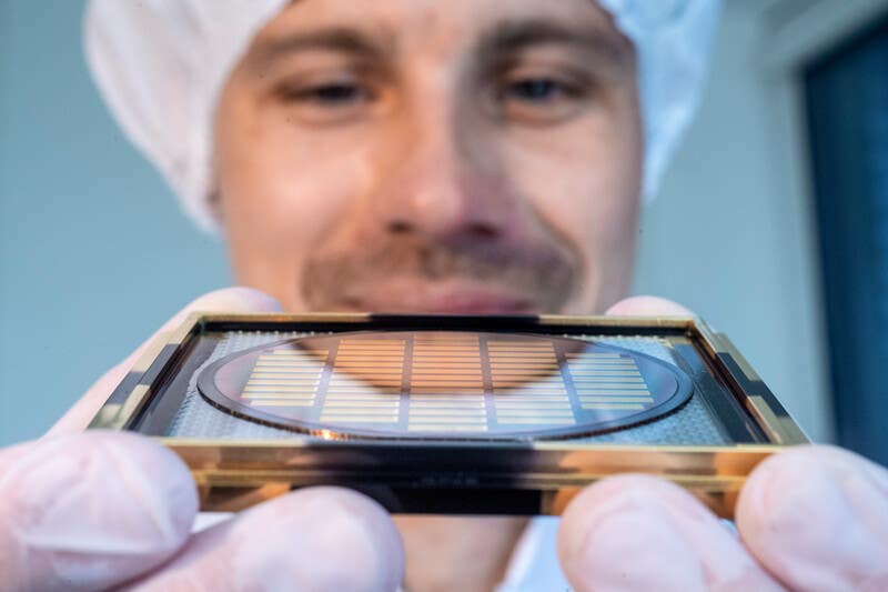
Photonic chips, using light instead of electricity, could reshape computing, delivering extraordinary efficiency and speed for AI technology. (CREDIT: Trumpf Group)
Artificial intelligence (AI) continues to shape your daily life, from online shopping to medical research. Yet behind every click or discovery is a hidden world of computing power facing tough challenges. Today's computers consume massive amounts of energy and generate heat, limiting their speed and efficiency. To tackle these problems, researchers have turned to a surprising solution: computing with light rather than electricity.
A recent breakthrough by Q.ANT, a German technology company, promises to redefine how AI chips are produced, leading the way to faster, greener, and more powerful computers worldwide.
A Groundbreaking Step Forward
At a high-tech facility in Stuttgart, engineers have unveiled a state-of-the-art production line dedicated exclusively to photonic AI chips. These chips use thin-film lithium niobate (TFLN), a special material ideal for managing light signals. This material makes it possible to control light waves extremely fast without generating excess heat.
By using existing semiconductor factories and upgrading them, the new approach significantly reduces costs and accelerates the development of AI processors. With an investment of €14 million, this innovation could reshape chip manufacturing globally, offering an example of how other countries might enhance their own tech production capabilities.
According to the CEO of the company behind this development, Dr. Michael Förtsch, this technology sets "a new benchmark for AI chip manufacturing," pointing toward greater energy efficiency and independence in semiconductor production.
How Photonic Chips Are Changing Computing
Photonic chips, also known as photonic neural processing units (NPUs), are cutting-edge processors that use light instead of electricity to perform computations. Unlike traditional electronic chips that rely on the movement of electrons through metal wires, photonic chips manipulate photons—particles of light—through waveguides, modulators, and other optical components etched into a silicon substrate.
This shift in medium allows photonic NPUs to perform certain calculations, especially those related to artificial intelligence (AI) and neural networks, much faster and more efficiently than conventional processors.
Related Stories
At the heart of a photonic NPU is the concept of optical interference. Light waves can be combined or canceled out depending on their phase and amplitude, and this property is used to perform matrix multiplications—core operations in AI workloads.
For example, when light passes through a network of programmable interferometers, it can be configured to represent weight matrices used in neural networks. The result of the interference patterns at the output corresponds to the computed data, effectively performing complex operations at the speed of light.
One major advantage of photonic chips is their ability to process multiple streams of data simultaneously through a technique called wavelength-division multiplexing. Each wavelength, or color, of light can carry its own stream of information, enabling high-throughput, parallel processing without the thermal and electrical limitations that slow down traditional chips. This means photonic NPUs can achieve extremely high bandwidth and lower latency while consuming far less energy.
Additionally, photonic chips are naturally suited for analog computation. Unlike digital electronics that break information into bits, photonic systems can represent and manipulate continuous values, which is useful for tasks like signal processing and AI inference. However, this also presents a challenge: maintaining accuracy and managing noise in analog optical systems is difficult, so hybrid designs that integrate both photonic and electronic components are often used.
Sustainable Computing Meets Practical Application
Photonic chips can achieve a 50-fold increase in processing speed while consuming 30 times less energy. This means that data centers, crucial for managing large-scale computing tasks, can run faster and more sustainably.
Dr. Förtsch highlights the critical need for this transition, noting, "As AI and data-intensive applications push conventional semiconductor technology to its limits, we need to rethink the way we approach computing at the core." Photonic processors offer exactly that, providing a sustainable solution to meet rising computing demands without overwhelming current infrastructure.
One major advantage of photonic chips is their ability to perform extremely fast optical signal adjustments at several gigahertz frequencies. Because they generate virtually no heat during these adjustments, they operate more accurately and efficiently than traditional chips made of silicon. This efficiency is essential for modern AI systems, which require intensive mathematical computations for tasks like machine learning, scientific simulations, and real-time data analysis.
Prof. Dr. Jens Anders, CEO of the semiconductor institute hosting the new production line, stresses that the new photonic chips set a "blueprint for energy-efficient next-generation computing." He emphasizes that now is the perfect time for such technology, as the rapid growth of AI and related applications soon risks overwhelming traditional data centers.
Real-world Benefits and Industry Implications
Beyond lab experiments, photonic chips are already demonstrating their potential through cloud-based AI trials. Integrated into existing data centers through standard PCIe interfaces, these processors can seamlessly boost current computing setups. They efficiently tackle key AI workloads such as model training, complex simulations, and high-density mathematical operations necessary in machine learning applications.
This technology does not seek to replace traditional processors like GPUs (graphics processing units), but rather to complement them, just as GPUs currently complement standard CPUs (central processing units). "We are not replacing GPUs – we are reshaping the next-generation compute ecosystem," Dr. Förtsch explains, underscoring photonics as the future standard for AI coprocessors.
The production line currently handles up to 1,000 wafers annually, allowing ongoing development and fine-tuning of chip designs. This facility also serves as a research hub for advanced server technology designed specifically for high-performance computing environments. Engineers and researchers can quickly adapt chip architecture to match evolving market needs, significantly speeding up the journey from lab to marketplace.
Six years ago, the team behind this innovation bet on TFLN technology. Today, that decision provides a distinct advantage. The combination of their expertise in photonics and complete control of the manufacturing process—from raw materials to finished products—positions them uniquely in the semiconductor industry. It also marks a critical step toward making high-speed, low-energy computing widely available and economically viable.
Accelerating Global Semiconductor Independence
Creating a blueprint for photonic chip production helps more than just one region or one company. It offers a model for other nations aiming to strengthen their semiconductor industries. Currently, global semiconductor production depends heavily on a few key regions. Any disruption can have severe consequences, affecting everything from car manufacturing to critical healthcare technologies.
This new photonic chip production method helps build independence from these global supply chains. Countries adopting similar manufacturing methods can produce their own advanced processors, enhancing resilience against future disruptions. This strategy offers a practical pathway toward a more distributed and stable semiconductor industry.
The company’s ultimate goal is ambitious yet clear: make photonic processors essential components in global AI infrastructure by 2030. "By 2030, we aim to make our photonic processors a scalable, energy-efficient cornerstone of AI infrastructure," Dr. Förtsch says, emphasizing the long-term commitment to reshaping technology sustainably.
The impact on computing will be transformative. Data centers will become cooler, faster, and significantly cheaper to operate. Scientific research and industry applications will accelerate, enabling innovations in medicine, climate modeling, and robotics to develop at unprecedented speeds.
Photonic Chips: The Future Begins Now
This breakthrough isn't just an incremental improvement—it's a dramatic shift. By harnessing the power of light, photonic processors promise to deliver substantial improvements in speed, efficiency, and sustainability. They represent not just better technology, but smarter technology, perfectly suited for an AI-driven future.
With photonic computing, the bottleneck of traditional chips could soon become a distant memory. As this technology scales and becomes mainstream, the possibilities for innovation are limitless. AI-driven industries, research institutions, and even your personal technology devices could soon experience dramatic leaps in speed and efficiency.
In a rapidly evolving digital world, photonic chips offer more than just technological advancement; they offer a clearer, brighter path to a sustainable computing future.
Note: The article above provided above by The Brighter Side of News.
Like these kind of feel good stories? Get The Brighter Side of News' newsletter.
Joshua Shavit
Science & Technology Writer | AI and Robotics Reporter
Joshua Shavit is a Los Angeles-based science and technology writer with a passion for exploring the breakthroughs shaping the future. As a contributor to The Brighter Side of News, he focuses on positive and transformative advancements in AI, technology, physics, engineering, robotics and space science. Joshua is currently working towards a Bachelor of Science in Business Administration at the University of California, Berkeley. He combines his academic background with a talent for storytelling, making complex scientific discoveries engaging and accessible. His work highlights the innovators behind the ideas, bringing readers closer to the people driving progress.