Silicon-photonic chip enables AI computing at light speed
Penn engineers have introduced a novel chip harnessing light waves, rather than electricity, to carry out intricate mathematical operations

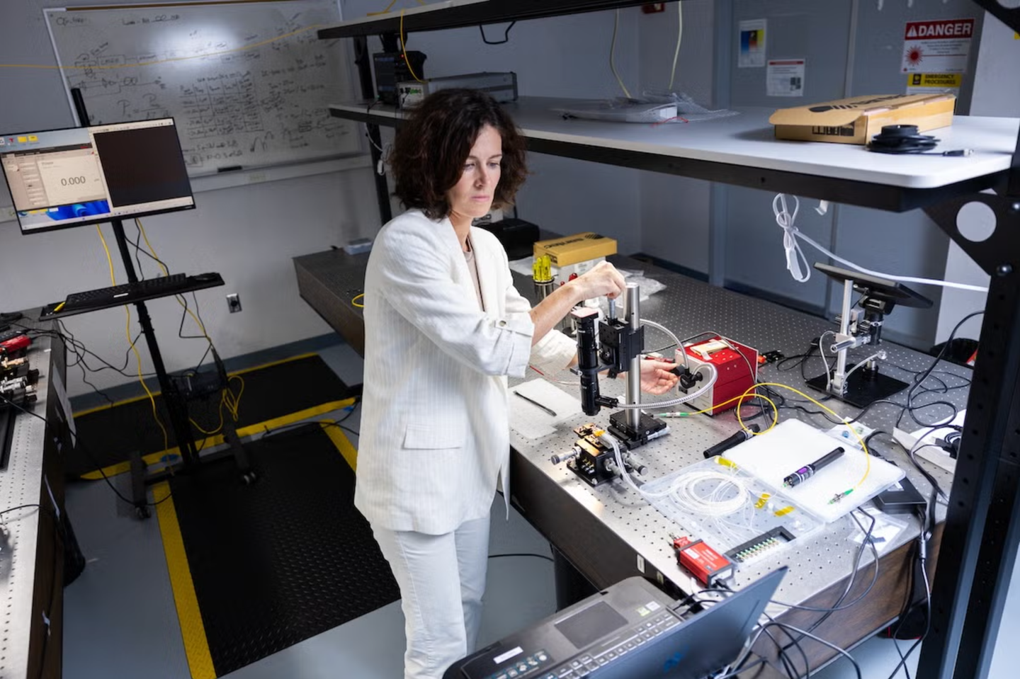
Penn engineers have introduced a novel chip harnessing light waves, rather than electricity, to carry out intricate mathematical operations vital for training AI. (CREDIT: Creative Commons)
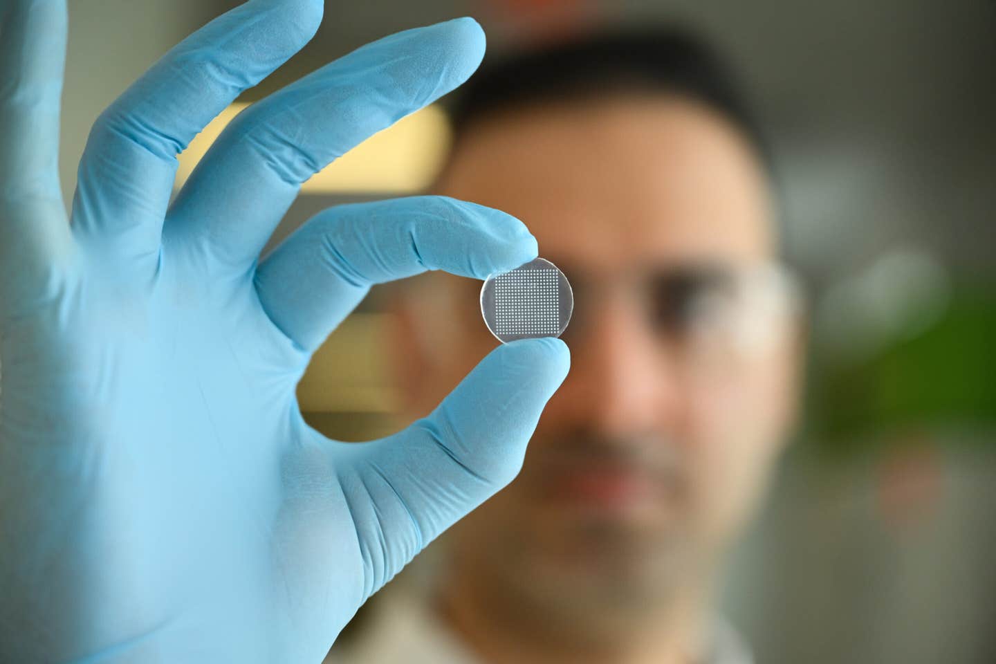
Penn engineers have introduced a novel chip harnessing light waves, rather than electricity, to carry out intricate mathematical operations vital for training AI. This innovation holds promise to drastically enhance computer processing speed while curbing energy consumption.
The silicon-photonic (SiPh) chip integrates the groundbreaking research of Benjamin Franklin Medal Laureate and H. Nedwill Ramsey Professor Nader Engheta.
Engheta's work focuses on manipulating materials at the nanoscale to execute mathematical computations using light, recognized as the swiftest mode of communication.
The chip merges Engheta's research with the SiPh platform, utilizing silicon, an abundant and cost-effective element extensively employed in mass-producing computer chips.
Related Stories
Exploring the interaction of light waves with matter offers a potential path to surpass the constraints of contemporary chips, rooted in principles dating back to the computing revolution's early days in the 1960s.
Published in Nature Photonics, a paper by Engheta's team in collaboration with Firooz Aflatouni, associate professor in electrical and systems engineering at Penn's School of Engineering and Applied Sciences, showcases their joint effort. Aflatouni's research group specializes in nanoscale silicon devices.
Their objective was to devise a platform capable of executing vector-matrix multiplication, a fundamental mathematical operation crucial for the development and operation of neural networks, the cornerstone of present-day AI tools.
Inverse-designed metastructures based on silicon photonics for performing 2 × 2 and 3 × 3 vector–matrix multiplications. (CREDIT: Nature Photonics)
Engheta explains, "Instead of using a silicon wafer of uniform height, you make the silicon thinner, say 150 nanometers," strategically varying the thickness only in specific regions.
These height discrepancies, devoid of additional materials, enable control over light propagation through the chip. The distribution of height variations induces specific light scattering patterns, empowering the chip to conduct mathematical computations at the speed of light.
Schematic of our inverse-designed structures in a SiPh platform. (CREDIT: Nature Photonics)
This study was conducted at the University of Pennsylvania School of Engineering and Applied science and supported in part by a grant from the U.S. Air Force Office of Scientific Research’s (AFOSR) Multidisciplinary University Research Initiative (MURI) to Engheta (FA9550-21-1-0312) and a grant from the U.S. Office of Naval Research (ONR) to Aflatouni (N00014-19-1-2248).
Additional co-authors include Vahid Nikkhah, Ali Pirmoradi, Farshid Ashtiani and Brian Edwards of Penn Engineering.
Note: Materials provided above by The Brighter Side of News. Content may be edited for style and length.
Like these kind of feel good stories? Get the Brighter Side of News' newsletter.


