Next-gen MRAM could replace DRAM chips in your next computer
Discover groundbreaking electric-field MRAM technology with reduced power consumption, enabling efficient, non-volatile memory for future computing.
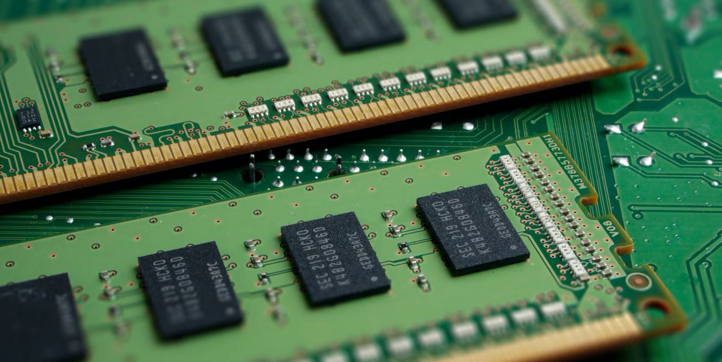
Researchers unveil electric-field MRAM technology, combining low power consumption and non-volatile data storage. Explore this innovation in memory devices. (CREDIT: CC BY-SA 4.0)
Memory technologies have seen rapid advancements as researchers strive to overcome the limitations of conventional systems. Magnetoresistive Random Access Memory (MRAM) stands out as a promising alternative to traditional volatile memory like DRAM.
Unlike DRAM, MRAM offers non-volatility, higher endurance, and compatibility with CMOS technology, making it a compelling option for applications demanding energy efficiency and reliability. Yet, a critical challenge remains: reducing energy consumption during the writing process.
Recent research published in the journal Advanced Science has explored new approaches to address this challenge, focusing on electric-field-based methods instead of conventional current-driven techniques.
A study published by Osaka University researchers demonstrates an innovative approach using a multiferroic heterostructure. This breakthrough significantly reduces energy requirements for data writing, advancing the potential of MRAM as a low-power memory technology.
Traditional MRAM systems rely on magnetization switching via spin-transfer torque (STT) or spin-orbit torque (SOT). These methods involve passing electric currents through heavy metals, such as platinum, tungsten, or tantalum. However, these current-driven techniques generate Joule heating, leading to substantial energy loss. While these methods have improved memory scaling and speed, the high power requirements remain a bottleneck for widespread adoption.
To overcome this limitation, electric-field (E)-based control of magnetization has been explored. This approach reduces power consumption by manipulating magnetization without relying on large currents. Initial efforts focused on ferromagnetic semiconductors and ultrathin ferromagnets on dielectric materials. However, these systems often required assistive magnetic fields, making them impractical for high-temperature applications.
In response, researchers have turned to multiferroic heterostructures comprising ferromagnetic and piezoelectric layers. These materials demonstrate robust performance above room temperature and offer diverse material combinations. They enable electric-field control of magnetization without external magnetic fields, presenting a viable pathway for energy-efficient MRAM development.
The Osaka University team achieved significant progress by developing a multiferroic heterostructure using a Heusler alloy (Co2FeSi) and a piezoelectric material (Pb(Mg1/3Nb2/3)O3-PbTiO3, or PMN-PT). A key innovation involved inserting an ultra-thin vanadium (V) layer between the ferromagnetic and piezoelectric layers. This insertion led to the growth of a highly oriented (422) Co2FeSi layer, which is crucial for achieving a giant converse magnetoelectric (CME) effect.
The CME effect describes how an applied electric field induces changes in magnetization. Larger CME coupling coefficients indicate stronger responses, and this study achieved coefficients exceeding 10⁻⁵ s/m. By carefully tuning the thickness of the vanadium and Co2FeSi layers, the researchers optimized magnetic anisotropy, enabling reliable electric-field control of the magnetization states.
Related Stories
Lead author Takamasa Usami explained, “As MRAM devices rely on a non-volatile magnetization state rather than a volatile charge state in capacitors, they are a promising alternative to DRAM in terms of their low power consumption in the standby state.”
The use of PMN-PT substrates, which exhibit strong piezoelectric properties, was integral to the research. These materials enable efficient strain transfer between the piezoelectric and ferromagnetic layers, facilitating electric-field-induced changes in magnetization. This approach contrasts with earlier methods that relied on high-temperature treatments, often degrading piezoelectric performance.
One of the most striking achievements of this study was the realization of non-volatile binary states at zero electric field. By manipulating the sweeping operation of the electric field, the researchers demonstrated two distinct magnetization states that remained stable without additional energy input. This property addresses a key requirement for practical MRAM devices, where stable data storage at minimal power consumption is essential.
The stability of these states stems from the precise growth of the (422) Co2FeSi layer, facilitated by the vanadium insertion. X-ray diffraction measurements confirmed the absence of structural fluctuations, ensuring consistent magnetic properties across the device. This advancement contrasts with previous designs that suffered from in-plane structural inconsistencies, limiting their reliability.
Additionally, scanning transmission electron microscopy (STEM) analysis provided insights into the atomic structure of the heterostructure. These images revealed a clear and uniform interface between the Co2FeSi and PMN-PT layers, underscoring the effectiveness of the vanadium insertion in promoting epitaxial growth.
Senior author Kohei Hamaya noted, “Through precise control of the multiferroic heterostructures, two key requirements for implementing practical magnetoelectric MRAM devices are satisfied, namely a non-volatile binary state with zero electric field, and a giant CME effect.”
The implications of this research extend beyond energy-efficient memory storage. The demonstrated multiferroic heterostructure not only reduces power consumption but also enhances the scalability and reliability of MRAM. By eliminating the need for large currents, the technology mitigates heat generation and material degradation, paving the way for durable memory devices.
Moreover, the integration of multiferroic heterostructures into existing manufacturing processes is a significant advantage. The compatibility of these materials with CMOS technology ensures that they can be incorporated into a wide range of electronic devices without requiring extensive redesigns.
The ability to achieve robust performance at room temperature and above makes these devices suitable for a wide range of applications, from consumer electronics to industrial systems. For instance, wearable medical devices, which demand both low power consumption and reliable performance, could greatly benefit from this technology.
This breakthrough also highlights the potential for magnetoelectric MRAM (ME-MRAM) as a transformative technology in spintronics. The combination of electric-field-driven switching and non-volatility aligns with the demands of modern computing, offering a sustainable alternative to energy-intensive memory solutions. Future developments could focus on further reducing the thickness of the ferromagnetic layers, enhancing speed, and minimizing power requirements even further.
As the Osaka University team continues to refine their design, the future of MRAM looks increasingly promising. The integration of multiferroic heterostructures into practical devices could revolutionize memory storage, enabling energy-efficient, high-capacity systems that meet the needs of next-generation computing. Additionally, the principles demonstrated in this study could inspire new approaches to other spintronic applications, including logic devices and sensors.
The work also underscores the importance of interdisciplinary collaboration in advancing memory technologies. By combining expertise in materials science, physics, and engineering, researchers have created a pathway toward sustainable and scalable solutions for the growing demands of digital storage.
Note: Materials provided above by The Brighter Side of News. Content may be edited for style and length.
Like these kind of feel good stories? Get The Brighter Side of News' newsletter.
Joshua Shavit
Science & Technology Writer | AI and Robotics Reporter
Joshua Shavit is a Los Angeles-based science and technology writer with a passion for exploring the breakthroughs shaping the future. As a contributor to The Brighter Side of News, he focuses on positive and transformative advancements in AI, technology, physics, engineering, robotics and space science. Joshua is currently working towards a Bachelor of Science in Business Administration at the University of California, Berkeley. He combines his academic background with a talent for storytelling, making complex scientific discoveries engaging and accessible. His work highlights the innovators behind the ideas, bringing readers closer to the people driving progress.