Millimeter-sized rare-earth crystal can hold terabytes of data
Scientists use rare-earth-doped crystals to store data at atomic scales, enabling high-density optical memory with low power consumption.
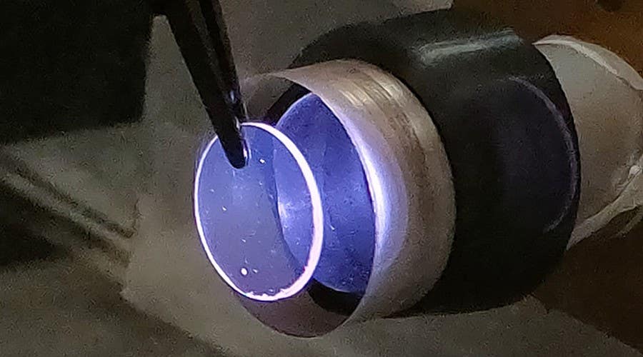
A crystal used in the study charges under UV light. The process created by Zhong Lab could be used with a variety of materials, taking advantage of rare earths’ powerful, flexible optical properties. (CREDIT: Zhong Lab)
The ability to store information has evolved from punch-card looms to modern smartphones. Every technological advancement has relied on defining states—on or off, high or low, pit or land—to encode data. Until now, the physical size of these storage elements has limited capacity.
Researchers at the University of Chicago's Pritzker School of Molecular Engineering have developed a method to store data at an atomic scale, using defects in rare-earth-doped crystals as memory units.
“Each memory cell is a single missing atom—a single defect,” said Tian Zhong, assistant professor at the university. “Now you can pack terabytes of bits within a small cube of material that’s only a millimeter in size.”
This discovery, published in Nanophotonics, leverages the optical properties of lanthanide-doped materials to create high-density memory storage. It represents a fusion of classical computing with quantum-inspired techniques, paving the way for efficient and scalable data retention.
Rare-Earth Elements and Crystal Defects
Rare-earth elements, also called lanthanides, have unique optical properties that make them ideal for applications in lasers, displays, and quantum computing. A common host for these elements is yttrium oxide (Y₂O₃), a stable metal oxide with a well-defined lattice structure. Within this matrix, rare-earth ions substitute constituent atoms, forming color centers.
However, metal oxides inherently contain lattice defects, such as missing oxygen atoms or interstitial oxygens. These defects can trap electrons and holes, creating stable charge states that influence the material’s electronic and optical behavior. The density of these charge traps depends on synthesis methods, growth conditions, and post-growth treatments.
In quantum information applications, these defects can pose challenges. They introduce charge noise, which impacts the quantum coherence of rare-earth ions used as quantum memories or emitters. Optical spectral diffusion, for example, broadens the linewidth of rare-earth ions due to interactions with fluctuating charge states. This effect is particularly noticeable in nanophotonic structures like waveguides and cavities.
Related Stories
To overcome these issues, researchers have developed optical charge trapping (OCT) spectroscopy, a technique that allows precise control of charge-trapping defects. By manipulating charge states, this method reduces local charge noise, improving optical coherence and enabling high-density optical storage.
Optical Charge Trapping and Memory Encoding
The experimental process begins with charging the sample using optical illumination at specific energy levels. The charge-trapping density is then measured through optically stimulated luminescence (OSL), a phenomenon in which trapped electrons recombine radiatively when stimulated by light. OSL has been widely used in luminescence dosimetry, persistent luminescence phosphors, and optical storage systems.
Using praseodymium (Pr³⁺)-doped Y₂O₃, researchers demonstrated that optical charging occurs through two main pathways:
- Inter-band transitions under ultraviolet (UV) excitation at 215 nm
- 4f-5d optical transitions at 275 nm within Pr³⁺ ions
Both processes are highly efficient, requiring optical intensities as low as 5 µW/cm². This low-power optical control allows for charge manipulation on demand, a crucial factor for scalable storage applications.
Unlike traditional memory storage, which relies on electrical signals, this technique encodes information through charge states in atomic-scale defects. A charged defect represents a "1," while an uncharged defect represents a "0." This allows a single millimeter cube of material to hold billions of classical memory bits.
From Radiation Dosimetry to Quantum-Inspired Storage
This research emerged from an unexpected source: radiation dosimetry. Lead author Leonardo França, a postdoctoral researcher in Zhong’s lab, initially studied materials that store radiation exposure data for medical and industrial applications. In hospitals and synchrotrons, dosimeters track radiation levels by capturing electron-hole pairs in crystal defects.
“In hospitals and particle accelerators, it’s essential to monitor how much radiation people are exposed to,” França explained. “Some materials absorb radiation and store that information for a certain amount of time.”
He discovered that shining light on these materials could release stored electrons, effectively "reading" the recorded data. This insight led him to explore its potential for data storage, bridging the gap between dosimetry and microelectronic memory.
By incorporating quantum-inspired techniques, the team developed a non-volatile optical memory system that combines principles from both classical and quantum information science. Unlike quantum computing, which relies on entangled qubits, this system remains firmly within the classical domain while benefiting from quantum-level precision in defect control.
“We're creating a new type of microelectronic device, a quantum-inspired technology,” Zhong said.
A Future for High-Density Optical Storage
Traditional memory storage devices, such as hard drives and flash memory, are reaching physical and thermal limitations. Shrinking transistors further is becoming increasingly difficult due to quantum tunneling effects at the nanoscale.
By using rare-earth-doped crystals, researchers have introduced an alternative storage medium with unparalleled density and stability. Since the charge-trapping process relies on optical means rather than electrical currents, these devices could also operate with lower power consumption and greater longevity.
The approach is highly adaptable. While the study used Pr³⁺ in a Y₂O₃ host, other rare-earth ions and crystal matrices could be employed, allowing customization for different optical properties and storage requirements.
“It’s well known that rare earths present specific electronic transitions that allow you to choose laser excitation wavelengths from UV up to near-infrared regimes,” França said.
This flexibility enables tailored solutions for next-generation optical memory and photonic computing applications. With further refinement, atomic-scale charge trapping could revolutionize how data is stored, from personal devices to large-scale cloud storage.
"Within that millimeter cube, we demonstrated there are at least a billion classical memories—traditional memories—based on atoms," Zhong said.
By harnessing defects that naturally exist in crystalline materials, this work turns imperfections into a powerful asset for data storage. With increasing demand for compact and efficient memory solutions, rare-earth-doped crystals may be the key to breaking conventional limits.
Note: Materials provided above by The Brighter Side of News. Content may be edited for style and length.
Like these kind of feel good stories? Get The Brighter Side of News' newsletter.
Rebecca Shavit
Science & Technology Journalist | Innovation Storyteller
Based in Los Angeles, Rebecca Shavit is a dedicated science and technology journalist who writes for The Brighter Side of News, an online publication committed to highlighting positive and transformative stories from around the world. With a passion for uncovering groundbreaking discoveries and innovations, she brings to light the scientific advancements shaping a better future. Her reporting spans a wide range of topics, from cutting-edge medical breakthroughs and artificial intelligence to green technology and space exploration. With a keen ability to translate complex concepts into engaging and accessible stories, she makes science and innovation relatable to a broad audience.